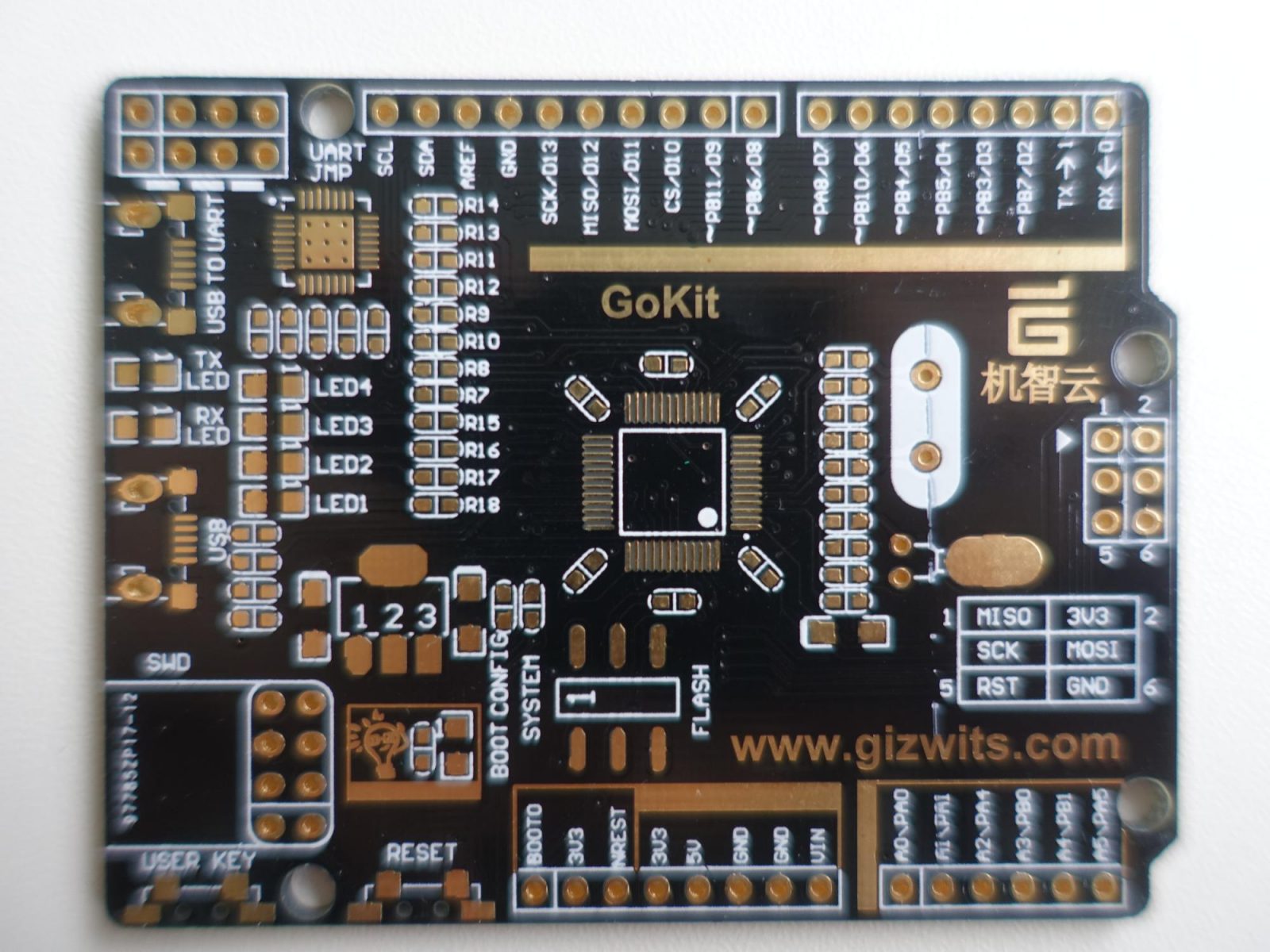
 Printed circuit board (PCB) inspection is a vital step in making certain quality and reliability throughout the electronics manufacturing course of. Both bare boards and assembled PCBs have to be carefully examined to validate acceptability before shipment to customers. But what specific standards constitute a proper PCB inspection? Read on for an overview of inspection objectives, standards, metrics, tools, and key defect sorts checked during the PCB inspection course of. Thorough inspection against established standards minimizes transport defective boards to customers. Manufacturers usually define an inspection plan with accept/reject criteria mapped to those requirements. IPC requirements in particular present a framework for decoding the severity of certain defects. Tracking metrics gives data to constantly improve processes and product high quality over time. Automated Optical Inspection (AOI) - Imaging system scans boards at high resolution capturing any defects. Computer algorithms analyze pictures in opposition to CAD information to detect discrepancies. Solder Mask Inspection - Validating uniformity and accuracy of solder mask software. Checking for voids, thin areas, misregistration.
Dimensional Inspection - Measuring crucial attributes like board thickness, lengths, hole positions. Confirming within specified tolerances. Hole Wall Integrity - Testing plated via-hole conductivity and plating quality using strategies like automated flying probe electrical testing. X-Ray Imaging - Captures defects inside boards like cracks, delamination, voiding, drilling errors. Thermal Stress Testing - Subjecting boards to thermal shock, cycling, and dwells reveals latent materials stresses and workmanship issues by means of failure analysis. Cross-Sectioning - Cutting micro-sections to examine plating thickness, resin fill, glass weave, and other inside board details below microscope. Bare board inspection focuses on design, fabrication, and material quality prior to elements being mounted. Bill of Materials (BOM) Accuracy - Confirming right parts installed in every designators position. Polarity - Verifying part orientation matches footprint polarity. Presence/Absence - Detecting lacking parts not mounted or incorrect portions. Component Value - Validating appropriate nominal worth components put in like correct resistor resistance or capacitor values.
Placement Accuracy - Checking location placement precision towards CAD centroid positions. Solder Joint Quality - Inspecting that solder fillets, toes, and bonds meet acceptability criteria. Foreign Object Debris (FOD) - Checking no loose particles, dirt, debris, or hair exists on the assembly. Mechanical Assembly - Ensuring no bent leads, visible damage, board warpage, discoloration, or scorching. Electrical Tests - Running in-circuit checks (ICT), boundary scans, and useful assessments to affirm correct electrical efficiency. Assembled board inspection focuses on parts, soldering, and functionality pre-shipment. Missing fine pitch marking. Automated Optical Inspection (AOI) - Vision cameras with sophisticated algorithms quickly scan boards against CAD fashions detecting discrepancies. Can examine solder joints, components, PCB options, markings, and extra. High throughput inline operation. Automated X-Ray Inspection (AXI) - X-ray imaging reveals hidden defects and confirms BOM, placement, and solder joint high quality with out destructive dismantling. Especially helpful for dens chips, BGAs, and QFNs. Solder Paste Inspection (SPI) - Validates volume, area, peak uniformity, and print registration of solder paste deposits by means of 3D optical metrology.
In-Circuit Test (ICT) - Electrical probes take a look at nodes throughout circuits verifying appropriate functionality. Fixtures allow repeatable probe alignment. Bed of Nails Test - Spring-loaded take a look at pins make electrical contact at testpoints across board checking continuity, shorts, and opens. Flying Probe Test - Automated probe mechanism touches down in any respect check nodes in a programmed sequence with out use of a fixture for electrical verification. Automated inspection replaces handbook visible checking with fast, goal, repeatable evaluation towards acceptance criteria thresholds. Every product usually maintains a personalized checklist primarily based on crucial characteristics and risks assessed from prior builds. What magnification is used to examine PCBs? Solder joints, machined features, and high-quality pitch parts require magnification. Handheld microscopes vary from 10x to over 100x. Machine imaginative and prescient cameras present up to 200x magnification. What are frequent PCB inspection failure points? Should you have almost any inquiries regarding wherever and also the way to work with PCB why, you possibly can call us in our web-page. Typical defects are thin/inadequate solder, missing or incorrect elements, poor solder fillets, pads lifted from board, scorched areas, flexed boards, and debris inclusions.
 How does automated optical inspection (AOI) work? AOI compares images of board options to CAD data using refined algorithms to identify discrepancies in the position, meeting, and soldering revealing any defects. Does PCB inspection influence manufacturing charge? Automated inspection integrates inline with out slowing total rate. Manual inspection can grow to be a bottleneck. AOI presents 10x the inspection points per hour compared to manual. What information ought to PCB inspection stories include? Reports convey images/details of each defect discovered, measurement knowledge, defect counts, process functionality metrics, repair suggestions, and move/fail status relative to acceptance criteria. Rigorous PCB inspection in opposition to established acceptability standards ensures high quality and reliability. Both naked boards and assembled PCBs endure intensive automated optical, electrical, and PCB why useful verification utilizing metrics defined by standards. Passing scrutiny throughout parameters like soldering, parts, board fabrication, and electrical operation supplies confidence prior to shipment. By institutionalizing robust inspection practices as a core self-discipline, electronics manufacturers cut back escapes, discipline failures, and guarantee customer satisfaction. It is strictly forbidden to directly take a look at the Tv, audio, video and different equipment without power isolation transformer with the equipment that's grounded.